Microelectronics
High-purity water is critical in manufacturing microelectronics for rinsing, cleaning, and etching semiconductor wafers. It removes contaminants and ensures the integrity of electronic components. Additionally, high-purity water serves as a coolant in various processes, preventing heat-induced damage. Its exceptional purity is essential for achieving precise and reliable performance in semiconductor fabrication.
Get A QuotePrecision Powered By Purity
The microelectronics industry is in a constant state of evolution, with demands for ultrapure water (UPW) becoming increasingly crucial to meet the exacting standards required for modern technologies. From complex computers to sophisticated military weaponry and everyday devices like computer monitors and cell phones, UPW is indispensable for achieving the high yields necessary to satisfy market demands. With manufacturing operations running 24/7/365, downtime is simply not an option.
Puretec stands at the forefront of UPW system design and manufacturing, boasting extensive experience in meeting the stringent requirements of the microelectronics industry. Our comprehensive UPW systems typically incorporate RO pretreatment, double-pass reverse osmosis (RO), primary ion exchange, advanced oxidation processes (AOP) such as UV, polishing ion exchange, and sub-micron filtration. Utilizing materials such as electropolished stainless steel and lubricant-free components, our systems ensure optimal purity and performance. With a service team equipped with decades of experience, Puretec remains dedicated to the maintenance and upkeep of these critical systems, evolving alongside the industry itself.
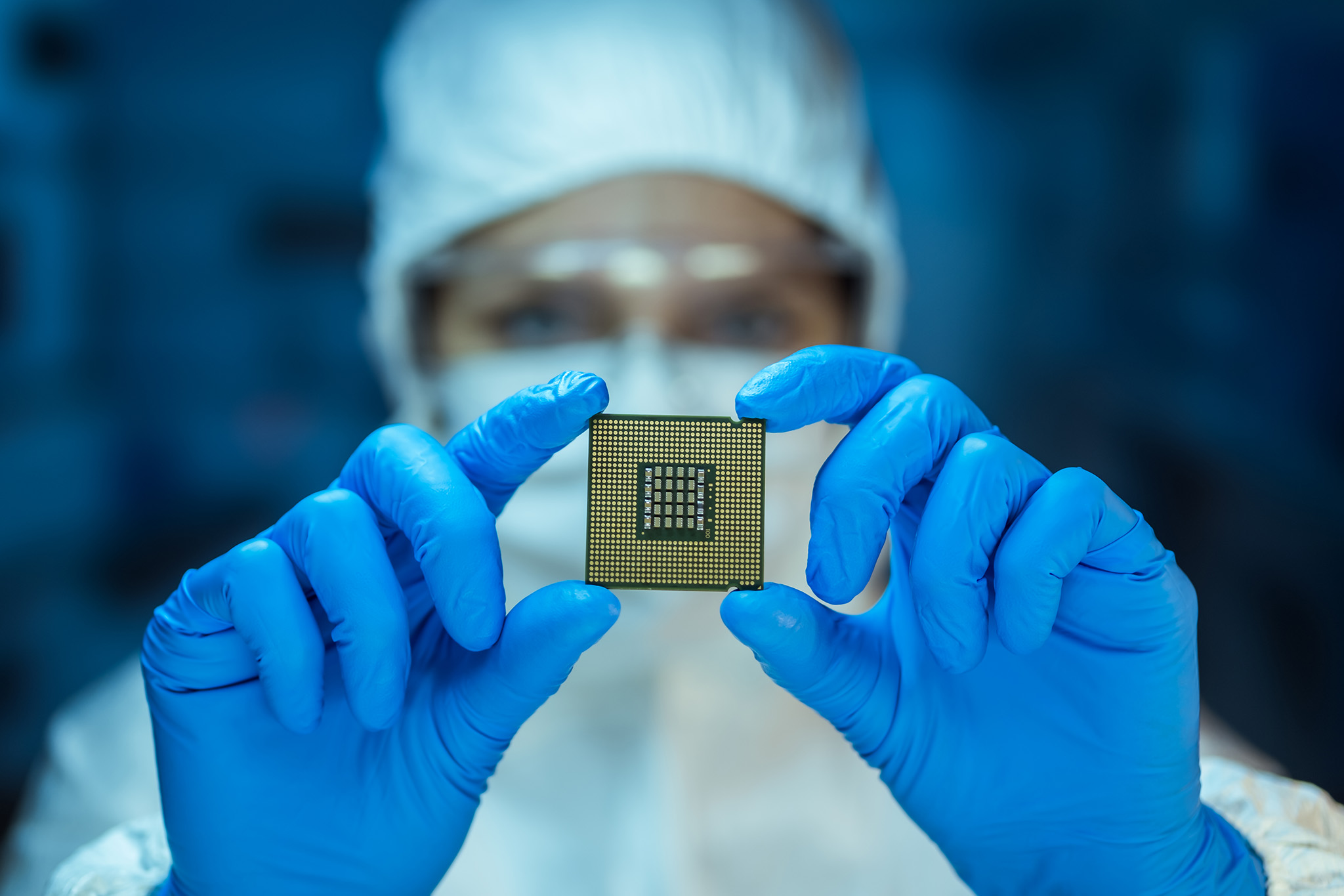
Semiconductors
The manufacturing of semiconductors requires multiple steps to apply transistor and circuit paths on a silicon wafer. In each step, ultrapure water is required to rinse impurities from the wafer surface. As manufacturing technology gets better and better and the circuitry gets smaller and smaller, water purity becomes extremely critical. Water-quality standards are defined by ASTM as Type E.1, Type E1.1, E1.2 with TOC, silica, boron, and particulate matter of the utmost importance.
Poor water quality poses significant challenges for semiconductor production, as even small contaminants can lead to defects and failures in electronic devices. Contaminants such as ions, particles, and organic compounds can interfere with semiconductor fabrication processes, causing defects in integrated circuits and reducing device performance and reliability. Additionally, poor water quality can contribute to equipment corrosion, fouling, and downtime, impacting manufacturing efficiency and yield. Ensuring high-quality water is essential for achieving the stringent purity requirements of semiconductor manufacturing and maintaining the integrity of electronic components.
Nanotechnology
Nanotechnology centers are state-of-the-art research facilities typically associated with universities and government entities. In microelectronics, their charter is to advance the technology wave forward, developing new materials and processes at the nanometer scale to further improve circuitry performance and reduce manufacturing costs. Water purity is critical to this research and typically mirrors the needs of semiconductor manufacturing, though on a smaller scale.
Nanotechnology offers exciting opportunities for revolutionary advancements in various fields, from electronics and medicine to energy and materials science. At the nanoscale, materials exhibit unique properties that can be harnessed for innovative applications, such as enhanced conductivity, increased strength, and targeted drug delivery. However, the production of nanomaterials presents challenges, including scalability, reproducibility, and cost-effectiveness. Achieving precise control over nanoscale structures and ensuring their uniformity on a large scale are key challenges in nanotechnology production, and high-purity water is at the core.